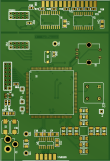
Altera FLEX 6024A Protoboard
During a lab cleanup at work I got four Altera FLEX 6024A FPGAs. These parts must have been samples that never made it into a product. They had a number of things going for them:
- Free,
- Obsolete (you can get CPLDs with more logic these days),
- In a PQ208 package, the same as the Altera Cyclone II I'm going to use in another project,
- So old that they only need a single voltage (3.3V).
Design
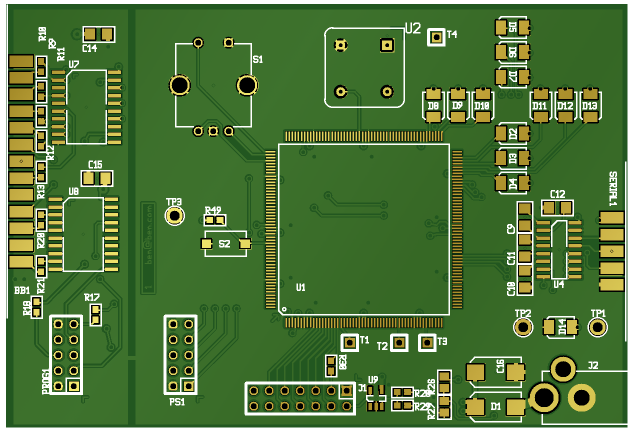
One of the first things I discovered is that Altera FPGAs of that vintage require a lot of help to configure. Altera made (or OEM'd) some specialized config proms that sequence the startup of the chip. Using them in a standalone configuration today would require buying parts that cost more than a modern FPGA. It made more sense to assume they'd be tethered to a PC, and just put a Byteblaster II clone on each board. That had the additional benefit of making the board useful even if the FPGA side was a flop.
At the beginning of the project I dreamed up a long list of possible peripherals to play with on the board. Then I ruthlessly pruned down to things I already had parts for (ideally scrounged), and that didn't involve a lot of investigation:
- A clock (in the form of a standard oscillator can, connected to one of the special clock pins),
- A reset button (connected to the special reset pin),
- A serial port with MAX3232 level shifter,
- Several LEDs of various colors in an interesting pattern,
- A rotary encoder with pushbutton (partly to test the footprint, as I was given many identical ones), and
- A standard 14 pin LCD header (with 5V power).
One edge of the board is taken up with a Byteblaster II clone (a standard Altera parallel programmer). It has a standard 10 pin connector which can be jumpered to an identical connector about 1" away on the main part of the board. The programmer can be used on other Altera boards as is, or it can be cut off the protoboard.
Schematic Capture and Layout
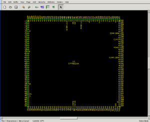 I'm still experimenting with gschem, and this time I decided to try a
different approach to symbol design and sheet layout.
Inspired by a
schematic for a Cyclone board made by Future Electronics, I made a
giant square symbol for the FPGA. The pins are all in the order you'd
find them in physically, but all of the ground and power pins have been
removed and are connected using
I'm still experimenting with gschem, and this time I decided to try a
different approach to symbol design and sheet layout.
Inspired by a
schematic for a Cyclone board made by Future Electronics, I made a
giant square symbol for the FPGA. The pins are all in the order you'd
find them in physically, but all of the ground and power pins have been
removed and are connected using net= attributes. The flex
part doesn't have many specialized pins, so mainly this is a big square
with "IO" all around it. I made this with
bjjboxsym from
a list of pins in the datasheet.
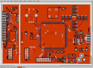
The schematic is one large sheet. I started by adding most of the parts and connecting all of the dedicated pins. From that I used gschem2pcb to build an initial PCB. I laid out a rectangle using wires to show the board outline in a much larger workspace. After playing with component arrangement for a while, I picked a dividing line for the programmer vs the FPGA side and created a ground plane for each on the top layer. Then I used a text editor to exactly clone those rectangles onto the bottom for the 3.3V power.
After I routed the nets I had already captured in the schematic, I started connecting the generic FPGA IOs to the peripherals using whatever was convenient for the placement and routing. This produces ratsnest errors in pcb in a format that is a handy report for capturing those nets in gschem. Another pass through gsch2pcb produces a new netlist which agrees with the nets already drawn on the board.
In the process of making this board I found several bugs in pcb, many of which I submitted to the tracker with fixes. I also made a pretty, hand-assembed PNG image of the board to try to inspire someone to improve pcb's PNG exporter.
A crucial step I missed was to make a pass over all of the elements to set a unified copper clearance and soldermask aperture.
Construction
I generated gerbers with pcb and scrutinized them with ViewMate to make sure they were correct and properly aligned. I had the boards professionally manufactured by Custom PCB in Kuala Lumpur, Malaysia. The cost was US$60 + $12 shipping for four identical, 2-sided boards with soldermask on both sides, but no silkscreen. I placed the order around midnight on Wednesday and the boards arrived the following Monday. I wasted no time assembling one!
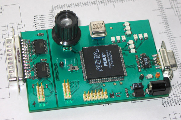
I assembled the Byteblaster II clone first and tried it with another Altera target. The Quartus II programmer detected it and was able to talk JTAG and AS. Then I assembled the two power supplies (3.3V main and a 5V for the LCD header) and verified that they worked before putting the FPGA on. With the FPGA and its programming header in place, I was able to configure the FPGA and know it was working. Then there was a mad scramble to solder on all the other parts! My test bitstream connected the serial port to the LCD and worked on the first try. No rework wires neeed!
Lessons Learned
One of my first lessons came very early in the design process. QFP leads are very fragile. Coupled with the fact that QFP soldering relies on proper registration of the leads just sitting on the pads, it is critical not to bend them in storage or transport. The leads are so close together that you can't even get the blunt side of an Xacto blade between them. You have to use the blade edge and align them very gently. If you transport a tray of QFP parts, make sure they're aligned properly in the tray and that the tray lid is attached securely. If a lead catches on a lip in the tray, you only have to bump the tray bend the it under the chip's own weight.
Beware the metric pin spacing. The pcb footprint library has many parts designed for the days when pcb's resolution was 1mil. The QFP208_28 footprint is one such part. On a fine-pitch metric land pattern, this leads to unevenly spaced pins. Pay attention to the quality of your footprints, and make your own if necessary.
Mind your soldermask. Current versions of pcb use square mask apertures and rounded copper clearances. If you flood the surfaces with copper, an equal sized (say, 10mil) mask and clearance will result in rounded arcs of the copper being exposed. See the detail of my 1200 DPI scan of the board. Plus, all fabs will have some registration tolerance which will prevent a mask from ever perfectly covering an equal sized copper feature. The mask should be a few mils smaller than the clearance (or 1/sqrt(2)*clearance, if your version of pcb is using square mask apertures).
Work with your vendor to choose pad geometries for close-tolerance components. One reason I paid extra for soldermask was to help with the QFP soldering. Since I did not consult them in advance, Custom PCB ganged the QFP pad apertures, leaving no mask between the pads. This turned out to be no problem for assembly, but with some advance planning I could have learned what geometry of pad and mask to use to preserve the individual pad masking.

