Reprogramming a JUMBO UNIVERSAL REMOTE...
...where by reprogramming I mean ripping out the old control circuitry and replacing it with a programmable microcontroller. If you found this page because you lost the tiny instruction booklet with the super-fine print (an ironic choice for a device with 1" tall buttons!), this is not the page you're looking for.
You should Buy a Logitech Harmony 670
 If you are interested in replicating this project, and your primary goal
is to have a nice universal remote, let me strongly encourage you
to go buy a
Logitech Harmony 670.
The behavior I've coded for this remote is directly inspired by the Harmony
I own for my primary entertainment center.
I don't work for Logitech, I'm
just a happy customer.
If you are interested in replicating this project, and your primary goal
is to have a nice universal remote, let me strongly encourage you
to go buy a
Logitech Harmony 670.
The behavior I've coded for this remote is directly inspired by the Harmony
I own for my primary entertainment center.
I don't work for Logitech, I'm
just a happy customer.
The genius of the Harmony series of remoes is that they are activity based rather than device based. On a typical univeral (or programmable) remote, when you select "DVD" the buttons on the remote all change to perform their DVD functions. You might hit "Power" then to turn on your DVD player. Then you'd select "TV" and turn it on as well. With the Harmony you choose "Watch Movie" and it turns on your DVD player, TV, receiver and any other devices you've told it are relevant. The buttons then each control the most obvious device. "Play" controls the DVD player, while "mute" controls the receiver and "Aspect" controls the TV. After I got mine, I really put all my other remotes away and had no urge to use them.
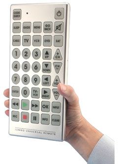
The JUMBO UNIVERSAL REMOTE
 An
IKEA EXPEDIT
entertainment center has become the home for all of my
game consoles and older AV equipment. The centerpiece of this new setup
is the 42" plasma panel display, which has an input and control board I
designed myself. The first-generation plasma has obvious shortcomings when
compared to modern HDTVs, but it's great for gaming. And of course having
designed the
display controller
myself it holds a special place in my heart.
Someday I'll write up that project.
An
IKEA EXPEDIT
entertainment center has become the home for all of my
game consoles and older AV equipment. The centerpiece of this new setup
is the 42" plasma panel display, which has an input and control board I
designed myself. The first-generation plasma has obvious shortcomings when
compared to modern HDTVs, but it's great for gaming. And of course having
designed the
display controller
myself it holds a special place in my heart.
Someday I'll write up that project.
What does all that have to do with the remote? What better remote for a giant flatscreen than a JUMBO UNIVERSAL REMOTE. As you can see from the picture on the right, it is truly jumbo. And you can find these everywhere on sale for about $15. Mine was an impulse buy at Fry's. Unfortunately, the only device I could get it to control at all was my old Panasonic DVD player.
Of course at that point there was nothing left to do but take it apart...
Disassembly
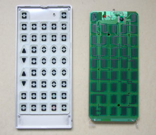 The case comes apart easily once you remove a few screws and squeeze the
bottom half of the case to release the locking tabs. It's so large that
the bits that needed to flex gave easily without risk of breaking. With
the case apart the PCB is removed from the front half. You can see the
battery terminals at the bottom of the PCB, which poke through the bottom
part of the case. The circutry is all at the top of the board (shown in
detail below).
The case comes apart easily once you remove a few screws and squeeze the
bottom half of the case to release the locking tabs. It's so large that
the bits that needed to flex gave easily without risk of breaking. With
the case apart the PCB is removed from the front half. You can see the
battery terminals at the bottom of the PCB, which poke through the bottom
part of the case. The circutry is all at the top of the board (shown in
detail below).
The PCB is a single layer with a second "layer" formed with conductive ink. The ink forms pads with interlocking fingers which are connected by button presses. The ink is also used to route crossing tracks over the single copper layer. The ink is fairly resistive so those bridges are mostly kept short.
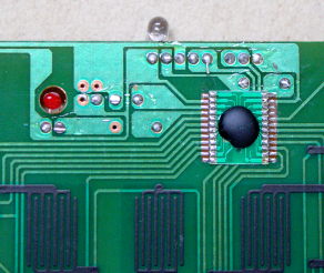
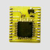
The best feature of the remote for hacking is that the brains are on a separate PCB mounted much like a SMT IC. There's a chip die with a blob of epoxy (common in cheap consumer devices) mounted on a carrier board. The board about 1/2 inch wide and the pads are spaced about 51mil. The PCB is very cheaply made, so it is tricky to remove this PCB without damaging it, as you will see. The single layer routing makes reverse- engineering the connections very easy.
 The board has a few discrete components mount on the back:
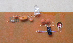
- The main IR LED in series with a ~1.5ohm resistor,
- A 4MHz ceramic resonator with two caps,
- A 100u electrolytic cap in parallel with a .1u ceramic across the power,
- A red indicator LED is in series with a 220 ohm resistor, and
- One pin on the IC is connected to a .1u to ground.
A Replacement Daughterboard
All features of the remote are controlled from the tiny "daughterboard" mounted on the main PCB. The entire behavior of the remote can be changed by replacing that tiny PCB. You could spend quite a bit of time selecting the ideal microcontroller to fit in the available space and meet the requirements of an IR remote design. Or you could do what I did, and use whatever you have on hand. In my case, the Atmel ATmega48 in TQFP32.
Luckily for me, the ATmega48 happens to be perfect for this application. Its features are a perfect match to the design challenges:
- It's small enough to fit (in the TQFP32 package),
- It will run directly on battery voltage,
- It has PWM outputs to simplify driving the IR LED,
- Weak pullups available on all IO pins eliminate the need for external pullup resistors and let me connect almost any pin to each edge connection, simplifying routing,
- It has a very low-power sleep mode,
- It supports pin-change interrupts on every IO, allowing me to spend more than 99% of the time sleeping between button presses, and again simplifying the PCB routing, and
- The only external help it needs is a transistor capable of pulsing the IR LED.
Reverse Engineering
Before I removed the old brains I gathered some data. I used a scope across the IR LED current limiting resistor to find the peak LED pulse current—about 185mA. The IR LED's Vf is about 1.8V.
Using a picture of the PCB in GIMP, I traced all of the nets connecting the matrix of buttons. There are two groups of nets, and each button is connected to a unique pair of those nets to allow presses to be detected by scanning. Once I had the nets drawn in color (very easy with shift-click to extend lines) I added a layer with a picture of the buttons and wrote down which nets each button was connected to. This gave me a pinout for the small daughtercard (if you look closely you can see its pin 1 is in the lower right on each of the above images).
Designing the Replacement
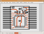 The
schematic
and
PCB were created with the free
gEDA suite of utilities.
You can download the project files.
I had already created a symbol for the ATmega48 and the MMBT3904 transistor,
and I created a new one to represent the edge connections of the PCB.
Keeping the PCB routing simple was the highest priority, so I used the
pinout display in PCB to see
which connections would be easiest to make. I then updated the schematic
to match my choices.
The
schematic
and
PCB were created with the free
gEDA suite of utilities.
You can download the project files.
I had already created a symbol for the ATmega48 and the MMBT3904 transistor,
and I created a new one to represent the edge connections of the PCB.
Keeping the PCB routing simple was the highest priority, so I used the
pinout display in PCB to see
which connections would be easiest to make. I then updated the schematic
to match my choices.
Because of the tight spacing and the single-layer design I needed all new footprints for my components in PCB. I adapted my QFP script to make a new TQFP32 footprint that's only a tiny bit larger than the actual chip. This makes it a little harder to solder, but gave me critical extra room to maneuver. I modified a 0603 footprint to have a 30mil gap in between the pads so I could use it to jump a 10/10 track. I made a footprint for the entire daughter card with extra long pads so I could trim the board to width after etching.
The replacement does not use the 4MHz crystal or the .1u cap pins available from the original PCB.
Construction
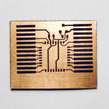 I made the board on thin (0.032) single-sided copper clad using the
toner transfer technique. I got
excellent results with the Brother HL-4070CDW, an affordable color
laser printer. On the right you can see the board after the toner transfer
and washing but before the etching and final trim. The fine traces are 10mil
including one that sneaks under an 0603 resistor.
I made the board on thin (0.032) single-sided copper clad using the
toner transfer technique. I got
excellent results with the Brother HL-4070CDW, an affordable color
laser printer. On the right you can see the board after the toner transfer
and washing but before the etching and final trim. The fine traces are 10mil
including one that sneaks under an 0603 resistor.
After etching I tinned the entire board with lots of flux and a soldering iron. Assembly was easy given that there are only 4 components! As always with QFP parts, use lots of water-soluble flux and it will be an easy job. Be sure to wash the board thoroughly with water when you're done because the flux residue will cause problems later.
The board as pictured does not match the board in the files linked from this page! I mistakenly used the RESET pin of the chip in my initial design. If you turn RESET into an IO it becomes impossible to program the chip in-circuit. I had to correct my mistake with a yellow wire you'll see below. The schematic and other files have been updated to use another pin, but the pictures of my construction include the mistake.
Brain Transplant
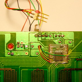
The trickiest part of the whole operation is removing the old chip. Whenever you desolder something there's a risk that you'll overheat the pads and cause them to delaminate. It's especially likely if you try to remove the part while it's still stuck to a pad. A quality PCB on a good laminate will give you a lot of leeway, but this is not a quality PCB. I tried to remove the board by cutting it in half with an xacto knife and desoldering each side with a "flood" of solder. I lifted several pads and even destroyed a few. I had to make a few connections by scraping off the soldermask and using a short wire.
I should have taken the board to work and used a hot air pencil to remove it. Chipquik would be another solution. The quick-and-dirty method might be to cut the traces on the old card and just attach the new one right on top. The epoxy blob might peel off to make that easier.
Once I had the old board off I cleaned the area underneath it and superglued my new board in place. Since the edges of the new board have no copper, you can't just solder it down like a chip. I took a stripped length of 30ga wire (kynar) about 3" long to attach the chip. At each pad on the new board I soldered on the wire. Then I used tweezers to push the wire down tightly against the side of the board and onto the base PCB pad. Then I cut it to length with an xacto knife (don't worry, you'd have to really saw to cut a trace on the board, just push straight down). Finally I tacked that wire to the pad on the base PCB. A few times the tiny wire would desolder from the daughterboard and I'd just wipe that wire off and start over.
If you can't manage the short wire method you could use short lenghts of wire looped over like the yellow one in the picture. That yellow wire corrects a mistake in the board (described above, and fixed in the downloadable files).
I used a Harbor Freight punch to make a hole for the ISP programming wires. Take care not to cut a trace! The wires are 30ga kynar soldered directly to the pins of the chip. There's not really room to bring them out to pads. The ISP header includes power and ground, which I got from two pre-existing holes (you can see them near the red LED). There's a pullup resistor attached to the programming header on the reset line. That should probably go on the board, but there's not really room. The ISP pigtail passes out of the enclosure through a hole in the bottom of the case. There's a tube-shaped reinforcement in the bottom and I used a forstner bit to open that tube to the outside. The header can tuck into the tube when it's not needed.
Programming
There's quite a bit for this section, but it's not done yet...

